
| Version 3 (modified by , 18 years ago) ( diff ) |
|---|
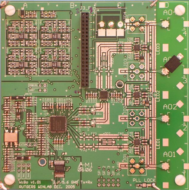
Orbit Noise Generator Wireless Board (WiBo)
WiBo102 is a 4.00 x 4.00” printed circuit board (PCB) designed around a Maxim, Inc. MAX2829ETN+D radio transceiver chip. This chip incorporates most of the radio functions except for the reference oscillator, baseband I/Q amps, power amps and antenna switches.
Four antennas (A01-A04) are mounted directly to WiBo102 though provision is made for adding SMA connectors and using off-board antennas if necessary. Two antennas are primarily for transmission (Tx) and two for receiving (Rx). Antenna switching is possible for diversity gain. It is also possible to switch all Tx and Rx signals into a single antenna.
- PCB
The PCB is a 4.00 x 4.00” FR-4 four-layer controlled impedance stackup board manufactured by Advanced Circuits, Inc.(http://www.4pcb.com/index.htm). For orientation purposes, reference marks are shown along the top (A-D) and right sides (1-4) of the board in one inch increments.
Looking from the top down, the top copper layer is the component side with all the high-frequency RF transmission lines. The dielectric under this layer is 20 mils thick. The structure of the traces is coplanar waveguide with ground (CPWG). A trace width of 30 mils and gap-to-ground of 18 mils provides a very close match to a 50ohm characteristic impedance.
The next copper layer down is all ground plane. The third layer down is a signal layer with predominately vertical traces surrounded by ground plane. The fourth or bottom layer is another signal layer with predominately horizontal traces.
BiBo’s ADC (analog-to-digital conversion) and DAC (digital-to-analog) conversion comes from an Analog Devices AD9860 MxFE processor. Digital RADIO_IO_x signals come from a Xilinx Spartan 3.
RADIO_IO_1/¾ download programming coefficients to the MAX2829.
RADIO_IO_3/4 are shared with U2 (74HC595), an 8bit serial in parallel out shift register. http://www.fairchildsemi.com/ds/MM/MM74HC595.pdf U2 in turn controls five functions, namely, turn on/off of the 2GHz and 5GHz power amps, MAX2829 RXENA and TXENA signals and the MAX2829 shutdown (/SHDN). Meaning of control signals
Assuming the MAX2829 has already been programmed, to enable a TX RF output the user must program a 11001xxx into U2.
NOTE! Do not turn on both the 2GHz and the 5GHz power amps at the same time! ALSO! Do not turn on both the RXENA and TXENA lines (not sure why?).
Connector J3_F and I/O
This is a 40-pin 2mm dual-inline connector which mates BiBo’s control signals, +3.3 VDC power and ground to WiBo102.
| WiBo102 function | J3_F function | pin# | pin# | J3_F function | WiBo102 function |
| hi-speed MAX2829 TXBBQ- | DACB- | 2 | 1 | 3.3VA | |
| hi-speed MAX2829 TXBBQ+ | DACB+ | 4 | 3 | GND | |
| hi-speed MAX2829 TXBBI- | DACA+ | 6 | 5 | 3.3VA | |
| hi-speed MAX2829 TXBBI+ | DACA- | 8 | 7 | GND | |
| phase modulation of U23 | AUX_DAC_C | 10 | 9 | 3.3VA | |
| ref osc VCXO frequency adjust | AUX_DAC_B | 12 | 11 | GND | |
| PLL speed up monitor | AUX_DAC_A | 14 | 13 | 3.3VA | |
| ½ supply voltage | AUX_ADC_A1 | 1 | 15 | GND | |
| RSSI from MAX2829 | AUX_ADC_A2 | 18 | 17 | N/C | |
| 2GHz power amp detector | AUX_ADC_B1 | 20 | 19 | 3.3VD | |
| 5GHz power amp detector | AUX_ADC_B2 | 22 | 21 | GND | |
| hi-speed MAX2829 RXI+ | ADCA+ | 24 | 23 | 3.3VD | |
| hi-speed MAX2829 RXI- | ADCA_ | 26 | 25 | GND | |
| hi-speed MAX2829 RXQ+ | ADCB+ | 28 | 27 | 3.3VD | |
| hi-speed MAX2829 RXQ- | ADCB- | 30 | 29 | GND | |
| MAX2829 /CS | RADIO_IO 1 | 32 | 31 | 3.3VD | |
| U2 RCK | RADIO_IO 2 | 34 | 33 | GND | |
| MAX2829 SCLK and U2 SCK | RADIO_IO 3 | 36 | 35 | RADIO_IO 8 | MAX2829 LD (lock=1=LED on) |
| MAX2829 DIN and U2 SER | RADIO_IO 4 | 38 | 37 | RADIO_IO 7 | U5 switch(straight=0,cross=1) |
| U3 switch(straight=0,cross=1) | RADIO_IO 5 | 40 | 39 | RADIO_IO 6 | U4 switch(straight=0,cross=1) |
Control Register U2
Note: A is the first bit in, so shift in reverse order
| 012345678 | Function |
| 1xxxxxxxx | turn MAX2829 on (/SHDN) |
| x1xxxxxxx | turn MAX2829 TX on (TXENA) |
| xx1xxxxxx | turn MAX2829 RX on (RXENA) |
| xxx1xxxxx | 5G PA: 5GHZ power amp on |
| xxxx1xxxx | 2G PA: 2GHz power amp on |
| xxxxx1xxx | SPARE 1 output on |
| xxxxxx1xx | SPARE 2 output on |
| xxxxxxx1x | SPARE 3 output on |
| xxxxxxxx1 | SPARE 4 output on, 9th bit |
Attachments (7)
- WiBo-103-Schematics.pdf (1.7 MB ) - added by 18 years ago.
-
MAX2828-9ds.pdf
(1.0 MB
) - added by 18 years ago.
Maxim Datasheet - UNDER NDA — NOT FOR DISTRIBUTION OUTSIDE WINLAB —
- MM74HC595.pdf (118.7 KB ) - added by 18 years ago.
- lt1994.pdf (288.1 KB ) - added by 18 years ago.
- uPG2035.pdf (148.2 KB ) - added by 18 years ago.
- AWL6951.pdf (671.0 KB ) - added by 18 years ago.
- WiBo-Photo.jpg (148.2 KB ) - added by 18 years ago.